


You are here:
Home » Products – Direct metallization
Direct metallization process
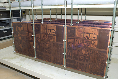
BECE CIRCuMET-DM2 – Palladium-based direct metallization process
Through-hole plating is one of the critical process steps in PCB manufacturing. Non-conductive hole walls must be prepared in such a way that uniform, adhesive, and process-reliable copper deposition is subsequently possible.
The BECE CIRCuMET-DM2 process is an economical direct metallization process for non-conductive substrates and enables the direct electrolytic deposition of copper onto palladium. It therefore offers an innovative and future-oriented alternative both to conventional electroless copper processes and to carbon-/graphite-based direct metallization processes.
Palladium-based direct metallization processes offer advantages over carbon-/graphite-based processes, particularly in terms of targeted activation of the hole wall surface and controlled preparation for the subsequent electrolytic copper deposition. While graphite-based systems rely on a conductive particle layer, palladium enables very fine and uniform catalytic activation, even on demanding surface structures. This can result in high process reliability, good copper bonding, and reliable through-hole plating — especially for modern PCB constructions, fine holes, HDI structures, and demanding base materials.
By using innovative, REACH- and RoHS-compliant additives in the process baths, the BECE CIRCuMET-DM2 process achieves a conductivity comparable to that of electroless copper processes.
The process can be applied in both horizontal and vertical processing lines.
Process sequence BECE CIRCuMET-DM2
Conditioning
Targeted surface modification to prepare the non-conductive areas.
Palladium activation
Activation of the hole wall as the basis for direct metallization.
Accelerator
Generates an even more active metal by modifying the adsorbed palladium colloid.
Electrolytic copper plating
Direct copper deposition onto the activated surface.
KEY PRODUCT ADVANTAGES:
- Continuous activation instead of particulate coating; uniform copper nucleation without local weaknesses.
- High process reliability for small holes; reliable even below 250 µm and with microvias.
- Wide process window; less dependence on drilling quality, wetting, and bath condition.
- HDI-capable and scalable; suitable for current and future design generations.
- Higher long-term reliability; reduced risk of voids and defects in electrolytic copper deposition.
- Excellent conductivity of the through-hole connections.
- Reliable electrolytic copper plating of non-conductors and all common substrates used in the PCB industry.
- Simple process control with a wide operating window.
- For horizontal and vertical applications.
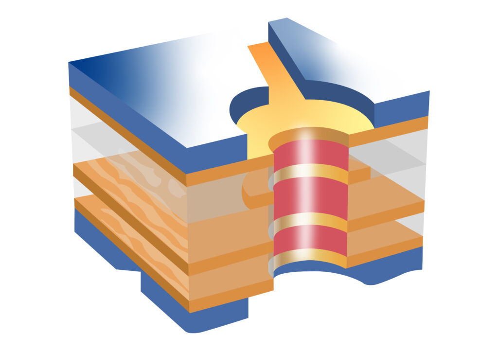
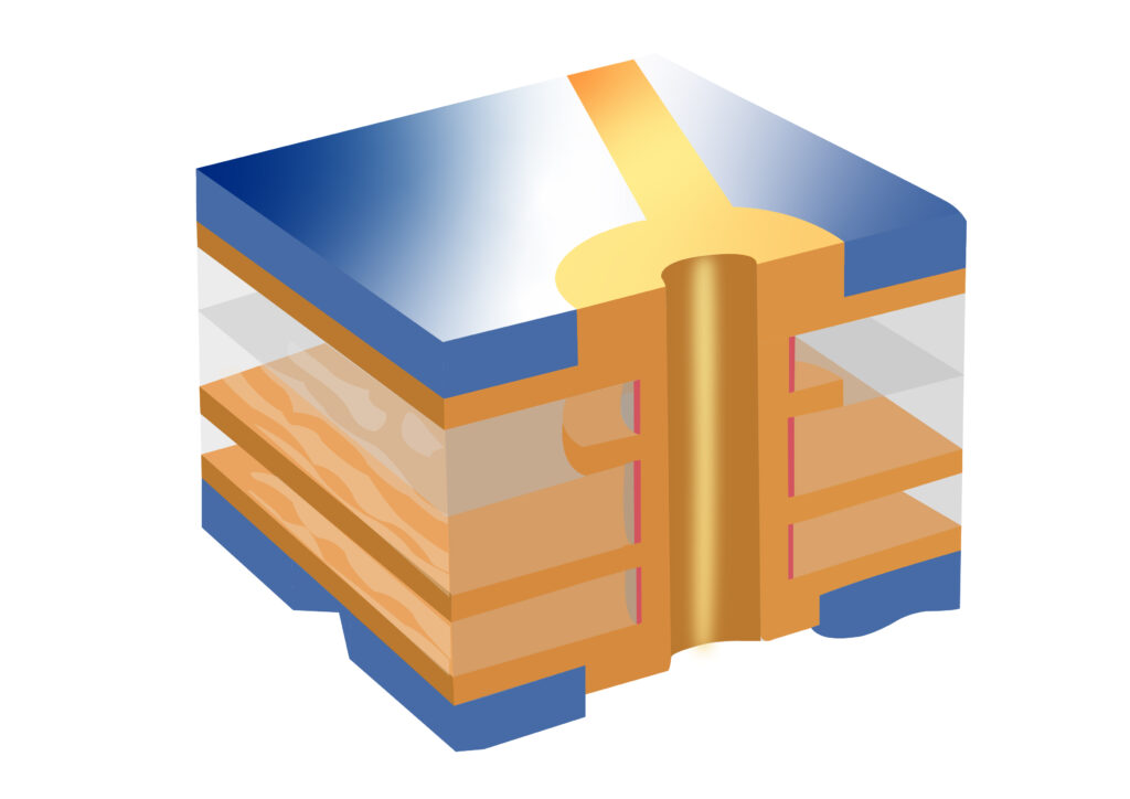
Visualization of Before and After: